Category: ℹ️ - Information
Parent channel: #⁉️-questions
Thread ID: 1498002344510492914
Messages: 24
message-1498002344510492914
2026-04-26T16:46:30.469+00:00 — namibj
- Message ID:
1498002344510492914 - Author ID:
262706220073222144 - Nickname: namibj
- User name: namibj
- Type:
Default - Discord message: https://discord.com/channels/1361349522684510449/1498002344510492914/1498002344510492914
- Archive source: https://discord.wafer.space/wafer-space/%E2%84%B9%EF%B8%8F%20-%20Information/%E2%81%89%EF%B8%8F-questions/possibility-of-soldering-to-lateral-gan/2026-04/2026-04.json
- Archive source: https://discord.wafer.space/wafer-space/Information/questions/possibility-of-soldering-to-lateral-gan/2026-04/2026-04.json
Content
Given the small size of these and need for low gate loop inductance, would it be feasible to overlap the gate pad are aof one of these over the edge of a WS die and have top metal structured to allow these to be soldered together?
I guess it would need some diffusion barrier plating stackup on top of the regular bond pad surface to prevent the top metal from just dissolving in the solder?
https://epc-co.com/epc/portals/0/epc/documents/datasheets/EPC8010_datasheet.pdf
Attachments
<details> <summary>Attachments data</summary>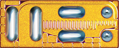
[
  {
    "fileName": "epc8010-die.png",
    "fileSizeBytes": 53224,
    "id": "1498002344674201843",
    "url": "2026-04_media/epc8010-die-A8809.png"
  }
]{
"author": {
"avatarUrl": "2026-04_media/f885abc0dddd0a33e4d4991b3c99091d-7ACD2.png",
"discriminator": "0000",
"isBot": false
},
"message": {}
}message-1498002451272433714
2026-04-26T16:46:55.923+00:00 — namibj
- Message ID:
1498002451272433714 - Author ID:
262706220073222144 - Nickname: namibj
- User name: namibj
- Type:
Default - Discord message: https://discord.com/channels/1361349522684510449/1498002344510492914/1498002451272433714
- Archive source: https://discord.wafer.space/wafer-space/%E2%84%B9%EF%B8%8F%20-%20Information/%E2%81%89%EF%B8%8F-questions/possibility-of-soldering-to-lateral-gan/2026-04/2026-04.json
- Archive source: https://discord.wafer.space/wafer-space/Information/questions/possibility-of-soldering-to-lateral-gan/2026-04/2026-04.json
Content
Attachments
<details> <summary>Attachments data</summary>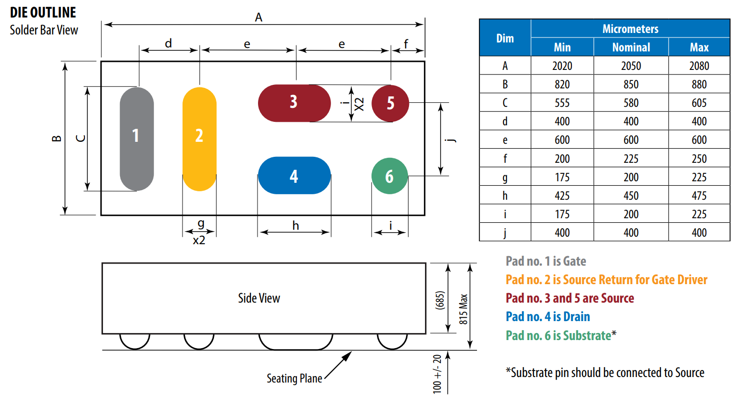
[
  {
    "fileName": "image.png",
    "fileSizeBytes": 127090,
    "id": "1498002450840555651",
    "url": "2026-04_media/image-A6471.png"
  }
]{
"author": {
"avatarUrl": "2026-04_media/f885abc0dddd0a33e4d4991b3c99091d-7ACD2.png",
"discriminator": "0000",
"isBot": false
},
"message": {}
}message-1498137132944851135
2026-04-27T01:42:06.536+00:00 — namibj
- Message ID:
1498137132944851135 - Author ID:
262706220073222144 - Nickname: namibj
- User name: namibj
- Type:
Default - Discord message: https://discord.com/channels/1361349522684510449/1498002344510492914/1498137132944851135
- Archive source: https://discord.wafer.space/wafer-space/%E2%84%B9%EF%B8%8F%20-%20Information/%E2%81%89%EF%B8%8F-questions/possibility-of-soldering-to-lateral-gan/2026-04/2026-04.json
- Archive source: https://discord.wafer.space/wafer-space/Information/questions/possibility-of-soldering-to-lateral-gan/2026-04/2026-04.json
Content
Rough math suggests gate drive currents under conditons of "clamp gate to gate-return, starting from a nicely charged gate" may peak at about 500 mA per such EPC8010, if that one is cooled well to support high operating currents and such nuances.
This stems from the mandate to keep the GaN chanel pinched off while the drain voltage rises from slightly above on-state (the gate driver won't turn on instantly, so it's better to start thinking from once the final output stage actually reaches full slew rate) to ful off-state operating voltage, with that speed governed by the LC "resonance" of the stray inductance discharging into the output capacitance of the GaN until the load current has fallen to zero.
So the limit is essentially defined by maximum operating load current and minimum guaranteed total drain charge for going from on-state to operating voltage.
The maximum current that this can reasonably sustain under excellent cooling and restriction to <=50% duty-cycle is about 5A; the datasheet specifies some 2.2 nC total drain charge for 50V situations.
That counters the approximately 0.3 nC of total gate charge required to slew from comfortably sustained saturation on-state gate voltage down below the miller plateu.{
"author": {
"avatarUrl": "2026-04_media/f885abc0dddd0a33e4d4991b3c99091d-7ACD2.png",
"discriminator": "0000",
"isBot": false
},
"message": {}
}message-1498188643700052109
2026-04-27T05:06:47.657+00:00 — Tim 'mithro' Ansell (@mithro_)
- Message ID:
1498188643700052109 - Author ID:
169786952432746498 - Nickname: Tim 'mithro' Ansell
- User name: mithro_
- Type:
Default - Discord message: https://discord.com/channels/1361349522684510449/1498002344510492914/1498188643700052109
- Archive source: https://discord.wafer.space/wafer-space/%E2%84%B9%EF%B8%8F%20-%20Information/%E2%81%89%EF%B8%8F-questions/possibility-of-soldering-to-lateral-gan/2026-04/2026-04.json
- Archive source: https://discord.wafer.space/wafer-space/Information/questions/possibility-of-soldering-to-lateral-gan/2026-04/2026-04.json
Content
@namibj - I suggest chatting with @Tim Edwards - I believe that he had some friends who where exploring how to do things like this.{
"author": {
"avatarUrl": "2026-04_media/9679bb77da48d47c905b398d98a83780-75B68.png",
"discriminator": "0000",
"isBot": false
},
"message": {
"mentions": [
{
"avatarUrl": "2026-04_media/f885abc0dddd0a33e4d4991b3c99091d-7ACD2.png",
"color": null,
"discriminator": "0000",
"id": "262706220073222144",
"isBot": false,
"name": "namibj",
"nickname": "namibj",
"roles": []
},
{
"avatarUrl": "2026-04_media/6bcc8e61db497b620550682309ace5d5-D89B4.png",
"color": null,
"discriminator": "0000",
"id": "1365118310701600900",
"isBot": false,
"name": "rtimothyedwards_19428",
"nickname": "Tim Edwards",
"roles": []
}
]
}
}message-1498188801422659726
2026-04-27T05:07:25.261+00:00 — Tim 'mithro' Ansell (@mithro_)
- Message ID:
1498188801422659726 - Author ID:
169786952432746498 - Nickname: Tim 'mithro' Ansell
- User name: mithro_
- Type:
Default - Discord message: https://discord.com/channels/1361349522684510449/1498002344510492914/1498188801422659726
- Archive source: https://discord.wafer.space/wafer-space/%E2%84%B9%EF%B8%8F%20-%20Information/%E2%81%89%EF%B8%8F-questions/possibility-of-soldering-to-lateral-gan/2026-04/2026-04.json
- Archive source: https://discord.wafer.space/wafer-space/Information/questions/possibility-of-soldering-to-lateral-gan/2026-04/2026-04.json
Content
They where doing high current direct die bonding or something similar.{
"author": {
"avatarUrl": "2026-04_media/9679bb77da48d47c905b398d98a83780-75B68.png",
"discriminator": "0000",
"isBot": false
},
"message": {}
}message-1498189486696169572
2026-04-27T05:10:08.643+00:00 — namibj
- Message ID:
1498189486696169572 - Author ID:
262706220073222144 - Nickname: namibj
- User name: namibj
- Type:
Reply - Discord message: https://discord.com/channels/1361349522684510449/1498002344510492914/1498189486696169572
- Archive source: https://discord.wafer.space/wafer-space/%E2%84%B9%EF%B8%8F%20-%20Information/%E2%81%89%EF%B8%8F-questions/possibility-of-soldering-to-lateral-gan/2026-04/2026-04.json
- Archive source: https://discord.wafer.space/wafer-space/Information/questions/possibility-of-soldering-to-lateral-gan/2026-04/2026-04.json
Reply/reference
<details> <summary>Reference data</summary>{
"channelId": "1498002344510492914",
"guildId": "1361349522684510449",
"messageId": "1498188801422659726"
}Content
sounds at least fairly closely related.{
"author": {
"avatarUrl": "2026-04_media/f885abc0dddd0a33e4d4991b3c99091d-7ACD2.png",
"discriminator": "0000",
"isBot": false
},
"message": {
"mentions": [
{
"avatarUrl": "2026-04_media/9679bb77da48d47c905b398d98a83780-75B68.png",
"color": null,
"discriminator": "0000",
"id": "169786952432746498",
"isBot": false,
"name": "mithro_",
"nickname": "Tim 'mithro' Ansell",
"roles": []
}
]
}
}message-1498189642930065468
2026-04-27T05:10:45.892+00:00 — namibj
- Message ID:
1498189642930065468 - Author ID:
262706220073222144 - Nickname: namibj
- User name: namibj
- Type:
Default - Discord message: https://discord.com/channels/1361349522684510449/1498002344510492914/1498189642930065468
- Archive source: https://discord.wafer.space/wafer-space/%E2%84%B9%EF%B8%8F%20-%20Information/%E2%81%89%EF%B8%8F-questions/possibility-of-soldering-to-lateral-gan/2026-04/2026-04.json
- Archive source: https://discord.wafer.space/wafer-space/Information/questions/possibility-of-soldering-to-lateral-gan/2026-04/2026-04.json
Content
https://epc-co.com/epc/portals/0/epc/documents/datasheets/EPC2019_datasheet.pdf btw is another possible "option" vs. the above one{
"author": {
"avatarUrl": "2026-04_media/f885abc0dddd0a33e4d4991b3c99091d-7ACD2.png",
"discriminator": "0000",
"isBot": false
},
"message": {}
}message-1498189753735184404
2026-04-27T05:11:12.31+00:00 — namibj
- Message ID:
1498189753735184404 - Author ID:
262706220073222144 - Nickname: namibj
- User name: namibj
- Type:
Default - Discord message: https://discord.com/channels/1361349522684510449/1498002344510492914/1498189753735184404
- Archive source: https://discord.wafer.space/wafer-space/%E2%84%B9%EF%B8%8F%20-%20Information/%E2%81%89%EF%B8%8F-questions/possibility-of-soldering-to-lateral-gan/2026-04/2026-04.json
- Archive source: https://discord.wafer.space/wafer-space/Information/questions/possibility-of-soldering-to-lateral-gan/2026-04/2026-04.json
Content
Attachments
<details> <summary>Attachments data</summary>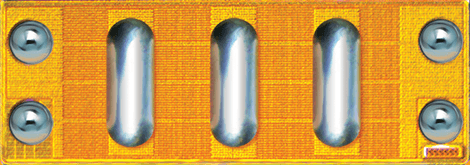
[
  {
    "fileName": "epc2019-die.png",
    "fileSizeBytes": 60982,
    "id": "1498189753433067581",
    "url": "2026-04_media/epc2019-die-FA19C.png"
  }
]{
"author": {
"avatarUrl": "2026-04_media/f885abc0dddd0a33e4d4991b3c99091d-7ACD2.png",
"discriminator": "0000",
"isBot": false
},
"message": {}
}message-1498189922715177071
2026-04-27T05:11:52.598+00:00 — namibj
- Message ID:
1498189922715177071 - Author ID:
262706220073222144 - Nickname: namibj
- User name: namibj
- Type:
Default - Discord message: https://discord.com/channels/1361349522684510449/1498002344510492914/1498189922715177071
- Archive source: https://discord.wafer.space/wafer-space/%E2%84%B9%EF%B8%8F%20-%20Information/%E2%81%89%EF%B8%8F-questions/possibility-of-soldering-to-lateral-gan/2026-04/2026-04.json
- Archive source: https://discord.wafer.space/wafer-space/Information/questions/possibility-of-soldering-to-lateral-gan/2026-04/2026-04.json
Content
0.95mm wide "bar"; top left ball source, bottom left bar gate.{
"author": {
"avatarUrl": "2026-04_media/f885abc0dddd0a33e4d4991b3c99091d-7ACD2.png",
"discriminator": "0000",
"isBot": false
},
"message": {}
}message-1498190099907739698
2026-04-27T05:12:34.844+00:00 — namibj
- Message ID:
1498190099907739698 - Author ID:
262706220073222144 - Nickname: namibj
- User name: namibj
- Type:
Default - Discord message: https://discord.com/channels/1361349522684510449/1498002344510492914/1498190099907739698
- Archive source: https://discord.wafer.space/wafer-space/%E2%84%B9%EF%B8%8F%20-%20Information/%E2%81%89%EF%B8%8F-questions/possibility-of-soldering-to-lateral-gan/2026-04/2026-04.json
- Archive source: https://discord.wafer.space/wafer-space/Information/questions/possibility-of-soldering-to-lateral-gan/2026-04/2026-04.json
Content
Attachments
<details> <summary>Attachments data</summary>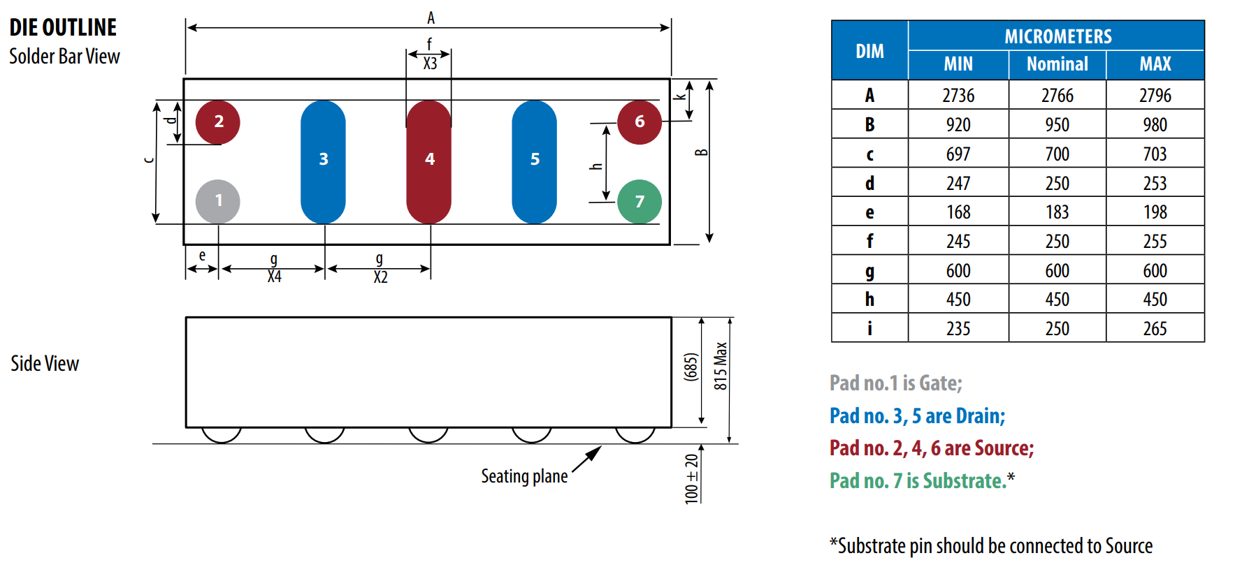
[
  {
    "fileName": "image.png",
    "fileSizeBytes": 158456,
    "id": "1498190099504955555",
    "url": "2026-04_media/image-86D5F.png"
  }
]{
"author": {
"avatarUrl": "2026-04_media/f885abc0dddd0a33e4d4991b3c99091d-7ACD2.png",
"discriminator": "0000",
"isBot": false
},
"message": {}
}message-1498190295140007976
2026-04-27T05:13:21.391+00:00 — namibj
- Message ID:
1498190295140007976 - Author ID:
262706220073222144 - Nickname: namibj
- User name: namibj
- Type:
Default - Discord message: https://discord.com/channels/1361349522684510449/1498002344510492914/1498190295140007976
- Archive source: https://discord.wafer.space/wafer-space/%E2%84%B9%EF%B8%8F%20-%20Information/%E2%81%89%EF%B8%8F-questions/possibility-of-soldering-to-lateral-gan/2026-04/2026-04.json
- Archive source: https://discord.wafer.space/wafer-space/Information/questions/possibility-of-soldering-to-lateral-gan/2026-04/2026-04.json
Content
tbf that one might take stronger objection to the source ball closest to the gate ball being used as a dedicated gate-return.{
"author": {
"avatarUrl": "2026-04_media/f885abc0dddd0a33e4d4991b3c99091d-7ACD2.png",
"discriminator": "0000",
"isBot": false
},
"message": {}
}message-1498191532719739061
2026-04-27T05:18:16.453+00:00 — namibj
- Message ID:
1498191532719739061 - Author ID:
262706220073222144 - Nickname: namibj
- User name: namibj
- Type:
Default - Discord message: https://discord.com/channels/1361349522684510449/1498002344510492914/1498191532719739061
- Archive source: https://discord.wafer.space/wafer-space/%E2%84%B9%EF%B8%8F%20-%20Information/%E2%81%89%EF%B8%8F-questions/possibility-of-soldering-to-lateral-gan/2026-04/2026-04.json
- Archive source: https://discord.wafer.space/wafer-space/Information/questions/possibility-of-soldering-to-lateral-gan/2026-04/2026-04.json
Content
(Some more reading meanwhile suggested that one might want to try bonding the opposite edge of the die normally as COB, adding that drop of resin to protect the bonds and act as passivation for the otherwise-exposed metal surfaces, and then do zincate pre-treatment folllowed with basically regular ENIG on exposed pads of suitable shape, before then doing mostly-normal reflow and ideally finishing with underfill to make up for the overhang-aspect.){
"author": {
"avatarUrl": "2026-04_media/f885abc0dddd0a33e4d4991b3c99091d-7ACD2.png",
"discriminator": "0000",
"isBot": false
},
"message": {}
}message-1498191593033826336
2026-04-27T05:18:30.833+00:00 — Tim 'mithro' Ansell (@mithro_)
- Message ID:
1498191593033826336 - Author ID:
169786952432746498 - Nickname: Tim 'mithro' Ansell
- User name: mithro_
- Type:
Default - Discord message: https://discord.com/channels/1361349522684510449/1498002344510492914/1498191593033826336
- Archive source: https://discord.wafer.space/wafer-space/%E2%84%B9%EF%B8%8F%20-%20Information/%E2%81%89%EF%B8%8F-questions/possibility-of-soldering-to-lateral-gan/2026-04/2026-04.json
- Archive source: https://discord.wafer.space/wafer-space/Information/questions/possibility-of-soldering-to-lateral-gan/2026-04/2026-04.json
Content
@namibj - You are welcome to put any type of pads on the top metal you want as long as it passes the DRC rules.{
"author": {
"avatarUrl": "2026-04_media/9679bb77da48d47c905b398d98a83780-75B68.png",
"discriminator": "0000",
"isBot": false
},
"message": {
"mentions": [
{
"avatarUrl": "2026-04_media/f885abc0dddd0a33e4d4991b3c99091d-7ACD2.png",
"color": null,
"discriminator": "0000",
"id": "262706220073222144",
"isBot": false,
"name": "namibj",
"nickname": "namibj",
"roles": []
}
]
}
}message-1498191663716368545
2026-04-27T05:18:47.685+00:00 — namibj
- Message ID:
1498191663716368545 - Author ID:
262706220073222144 - Nickname: namibj
- User name: namibj
- Type:
Default - Discord message: https://discord.com/channels/1361349522684510449/1498002344510492914/1498191663716368545
- Archive source: https://discord.wafer.space/wafer-space/%E2%84%B9%EF%B8%8F%20-%20Information/%E2%81%89%EF%B8%8F-questions/possibility-of-soldering-to-lateral-gan/2026-04/2026-04.json
- Archive source: https://discord.wafer.space/wafer-space/Information/questions/possibility-of-soldering-to-lateral-gan/2026-04/2026-04.json
Content
yeah but they're aluminium surface, right?{
"author": {
"avatarUrl": "2026-04_media/f885abc0dddd0a33e4d4991b3c99091d-7ACD2.png",
"discriminator": "0000",
"isBot": false
},
"message": {}
}message-1498191835384910016
2026-04-27T05:19:28.614+00:00 — Tim 'mithro' Ansell (@mithro_)
- Message ID:
1498191835384910016 - Author ID:
169786952432746498 - Nickname: Tim 'mithro' Ansell
- User name: mithro_
- Type:
Default - Discord message: https://discord.com/channels/1361349522684510449/1498002344510492914/1498191835384910016
- Archive source: https://discord.wafer.space/wafer-space/%E2%84%B9%EF%B8%8F%20-%20Information/%E2%81%89%EF%B8%8F-questions/possibility-of-soldering-to-lateral-gan/2026-04/2026-04.json
- Archive source: https://discord.wafer.space/wafer-space/Information/questions/possibility-of-soldering-to-lateral-gan/2026-04/2026-04.json
Content
@namibj - It would be super interesting to see if we could figure out a process/standard to put balls/solder directly onto the top metal pads in some way.....{
"author": {
"avatarUrl": "2026-04_media/9679bb77da48d47c905b398d98a83780-75B68.png",
"discriminator": "0000",
"isBot": false
},
"message": {
"mentions": [
{
"avatarUrl": "2026-04_media/f885abc0dddd0a33e4d4991b3c99091d-7ACD2.png",
"color": null,
"discriminator": "0000",
"id": "262706220073222144",
"isBot": false,
"name": "namibj",
"nickname": "namibj",
"roles": []
}
]
}
}message-1498191857505669171
2026-04-27T05:19:33.888+00:00 — Tim 'mithro' Ansell (@mithro_)
- Message ID:
1498191857505669171 - Author ID:
169786952432746498 - Nickname: Tim 'mithro' Ansell
- User name: mithro_
- Type:
Reply - Discord message: https://discord.com/channels/1361349522684510449/1498002344510492914/1498191857505669171
- Archive source: https://discord.wafer.space/wafer-space/%E2%84%B9%EF%B8%8F%20-%20Information/%E2%81%89%EF%B8%8F-questions/possibility-of-soldering-to-lateral-gan/2026-04/2026-04.json
- Archive source: https://discord.wafer.space/wafer-space/Information/questions/possibility-of-soldering-to-lateral-gan/2026-04/2026-04.json
Reply/reference
<details> <summary>Reference data</summary>{
"channelId": "1498002344510492914",
"guildId": "1361349522684510449",
"messageId": "1498191663716368545"
}Content
I believe so.{
"author": {
"avatarUrl": "2026-04_media/9679bb77da48d47c905b398d98a83780-75B68.png",
"discriminator": "0000",
"isBot": false
},
"message": {
"mentions": [
{
"avatarUrl": "2026-04_media/f885abc0dddd0a33e4d4991b3c99091d-7ACD2.png",
"color": null,
"discriminator": "0000",
"id": "262706220073222144",
"isBot": false,
"name": "namibj",
"nickname": "namibj",
"roles": []
}
]
}
}message-1498193013942259732
2026-04-27T05:24:09.604+00:00 — namibj
- Message ID:
1498193013942259732 - Author ID:
262706220073222144 - Nickname: namibj
- User name: namibj
- Type:
Reply - Discord message: https://discord.com/channels/1361349522684510449/1498002344510492914/1498193013942259732
- Archive source: https://discord.wafer.space/wafer-space/%E2%84%B9%EF%B8%8F%20-%20Information/%E2%81%89%EF%B8%8F-questions/possibility-of-soldering-to-lateral-gan/2026-04/2026-04.json
- Archive source: https://discord.wafer.space/wafer-space/Information/questions/possibility-of-soldering-to-lateral-gan/2026-04/2026-04.json
Reply/reference
<details> <summary>Reference data</summary>{
"channelId": "1498002344510492914",
"guildId": "1361349522684510449",
"messageId": "1498191835384910016"
}Content
to be clear I was "planning" to use the GaN die's WLCSP balls/bars to do a cantilever-arranged flip-chip setup, where the overhanging part of the GaN die has the drain and high-current-source pads that get soldered to a substrate "slab" _right_ next to the wafer.space die's edge, with just thermal expansion/dicing margin left between.
I mathed a little and it seems it's fairly practical to "just" dump large area MIM cap through a high-side switch into the GaN gate to rapidly turn it on; turn-off is obviously just shorting out the GaN's gate to the gate-return with an open-drain nmos array.{
"author": {
"avatarUrl": "2026-04_media/f885abc0dddd0a33e4d4991b3c99091d-7ACD2.png",
"discriminator": "0000",
"isBot": false
},
"message": {
"mentions": [
{
"avatarUrl": "2026-04_media/9679bb77da48d47c905b398d98a83780-75B68.png",
"color": null,
"discriminator": "0000",
"id": "169786952432746498",
"isBot": false,
"name": "mithro_",
"nickname": "Tim 'mithro' Ansell",
"roles": []
}
]
}
}message-1498193469670428740
2026-04-27T05:25:58.258+00:00 — namibj
- Message ID:
1498193469670428740 - Author ID:
262706220073222144 - Nickname: namibj
- User name: namibj
- Type:
Reply - Discord message: https://discord.com/channels/1361349522684510449/1498002344510492914/1498193469670428740
- Archive source: https://discord.wafer.space/wafer-space/%E2%84%B9%EF%B8%8F%20-%20Information/%E2%81%89%EF%B8%8F-questions/possibility-of-soldering-to-lateral-gan/2026-04/2026-04.json
- Archive source: https://discord.wafer.space/wafer-space/Information/questions/possibility-of-soldering-to-lateral-gan/2026-04/2026-04.json
Reply/reference
<details> <summary>Reference data</summary>{
"channelId": "1498002344510492914",
"guildId": "1361349522684510449",
"messageId": "1498189753735184404"
}Content
for scale, this one has approximately 5x the gate charge vs. the smaller faster one above.
That smaller one appears to just quite heavily limit it's active area for reasons I don't quite understand; there should be space for far higher saturation current at that breakdown voltage on that size die.{
"author": {
"avatarUrl": "2026-04_media/f885abc0dddd0a33e4d4991b3c99091d-7ACD2.png",
"discriminator": "0000",
"isBot": false
},
"message": {}
}message-1498193716408746094
2026-04-27T05:26:57.085+00:00 — namibj
- Message ID:
1498193716408746094 - Author ID:
262706220073222144 - Nickname: namibj
- User name: namibj
- Type:
Default - Discord message: https://discord.com/channels/1361349522684510449/1498002344510492914/1498193716408746094
- Archive source: https://discord.wafer.space/wafer-space/%E2%84%B9%EF%B8%8F%20-%20Information/%E2%81%89%EF%B8%8F-questions/possibility-of-soldering-to-lateral-gan/2026-04/2026-04.json
- Archive source: https://discord.wafer.space/wafer-space/Information/questions/possibility-of-soldering-to-lateral-gan/2026-04/2026-04.json
Content
the bottom one is approximately 50% more area but 400% more current _despite_ also having twice the breakdown voltage.{
"author": {
"avatarUrl": "2026-04_media/f885abc0dddd0a33e4d4991b3c99091d-7ACD2.png",
"discriminator": "0000",
"isBot": false
},
"message": {}
}message-1498195329508708456
2026-04-27T05:33:21.678+00:00 — namibj
- Message ID:
1498195329508708456 - Author ID:
262706220073222144 - Nickname: namibj
- User name: namibj
- Type:
Reply - Discord message: https://discord.com/channels/1361349522684510449/1498002344510492914/1498195329508708456
- Archive source: https://discord.wafer.space/wafer-space/%E2%84%B9%EF%B8%8F%20-%20Information/%E2%81%89%EF%B8%8F-questions/possibility-of-soldering-to-lateral-gan/2026-04/2026-04.json
- Archive source: https://discord.wafer.space/wafer-space/Information/questions/possibility-of-soldering-to-lateral-gan/2026-04/2026-04.json
Reply/reference
<details> <summary>Reference data</summary>{
"channelId": "1498002344510492914",
"guildId": "1361349522684510449",
"messageId": "1498191835384910016"
}Content
If you're ina a convenient position consider asking the bonding house if they do/can recommend someone who does do selective pad metallization; ENEPIG should also be an option (just a minor premium vs. ENIG) that retains the ability to do the wire bonding COB to such-plated pads; that would allow the chips which get such flip-chip soldering to undergo non-selective plating before they meet the wire bonder.
I don't see a reason why it should not work post-dicing; the chips might need to be attached to a carrier for handling in the plating system, though.

As this doesn't involve the traditional WLCSP mask layers it has good potential to scale down to the small batches we'd have.{
"author": {
"avatarUrl": "2026-04_media/f885abc0dddd0a33e4d4991b3c99091d-7ACD2.png",
"discriminator": "0000",
"isBot": false
},
"message": {
"mentions": [
{
"avatarUrl": "2026-04_media/9679bb77da48d47c905b398d98a83780-75B68.png",
"color": null,
"discriminator": "0000",
"id": "169786952432746498",
"isBot": false,
"name": "mithro_",
"nickname": "Tim 'mithro' Ansell",
"roles": []
}
]
}
}message-1498201534503059486
2026-04-27T05:58:01.064+00:00 — Tim 'mithro' Ansell (@mithro_)
- Message ID:
1498201534503059486 - Author ID:
169786952432746498 - Nickname: Tim 'mithro' Ansell
- User name: mithro_
- Type:
Default - Discord message: https://discord.com/channels/1361349522684510449/1498002344510492914/1498201534503059486
- Archive source: https://discord.wafer.space/wafer-space/%E2%84%B9%EF%B8%8F%20-%20Information/%E2%81%89%EF%B8%8F-questions/possibility-of-soldering-to-lateral-gan/2026-04/2026-04.json
- Archive source: https://discord.wafer.space/wafer-space/Information/questions/possibility-of-soldering-to-lateral-gan/2026-04/2026-04.json
Content
@namibj - Depend on how much funds you have, you could hire @stuart to see if he can find options for you in China. He is the person who is currently helping wafer.space get the wire bonding done.{
"author": {
"avatarUrl": "2026-04_media/9679bb77da48d47c905b398d98a83780-75B68.png",
"discriminator": "0000",
"isBot": false
},
"message": {
"mentions": [
{
"avatarUrl": "2026-04_media/f885abc0dddd0a33e4d4991b3c99091d-7ACD2.png",
"color": null,
"discriminator": "0000",
"id": "262706220073222144",
"isBot": false,
"name": "namibj",
"nickname": "namibj",
"roles": []
},
{
"avatarUrl": "2026-04_media/4938353f83780f56050d92be930226f8-BA286.png",
"color": null,
"discriminator": "0000",
"id": "1184268085822238821",
"isBot": false,
"name": "saladchap",
"nickname": "stuart",
"roles": []
}
]
}
}message-1498202414245740615
2026-04-27T06:01:30.811+00:00 — namibj
- Message ID:
1498202414245740615 - Author ID:
262706220073222144 - Nickname: namibj
- User name: namibj
- Type:
Default - Discord message: https://discord.com/channels/1361349522684510449/1498002344510492914/1498202414245740615
- Archive source: https://discord.wafer.space/wafer-space/%E2%84%B9%EF%B8%8F%20-%20Information/%E2%81%89%EF%B8%8F-questions/possibility-of-soldering-to-lateral-gan/2026-04/2026-04.json
- Archive source: https://discord.wafer.space/wafer-space/Information/questions/possibility-of-soldering-to-lateral-gan/2026-04/2026-04.json
Content
next year, then, I guess.{
"author": {
"avatarUrl": "2026-04_media/f885abc0dddd0a33e4d4991b3c99091d-7ACD2.png",
"discriminator": "0000",
"isBot": false
},
"message": {}
}message-1498330793313833041
2026-04-27T14:31:38.766+00:00 — namibj
- Message ID:
1498330793313833041 - Author ID:
262706220073222144 - Nickname: namibj
- User name: namibj
- Type:
Reply - Discord message: https://discord.com/channels/1361349522684510449/1498002344510492914/1498330793313833041
- Archive source: https://discord.wafer.space/wafer-space/%E2%84%B9%EF%B8%8F%20-%20Information/%E2%81%89%EF%B8%8F-questions/possibility-of-soldering-to-lateral-gan/2026-04/2026-04.json
- Archive source: https://discord.wafer.space/wafer-space/Information/questions/possibility-of-soldering-to-lateral-gan/2026-04/2026-04.json
Reply/reference
<details> <summary>Reference data</summary>{
"channelId": "1498002344510492914",
"guildId": "1361349522684510449",
"messageId": "1498201534503059486"
}Content
@stuart I mean I am open to consider sponsoring some searching for affordable flip-chip mounting of wafer.space dies; I'd assume there'd be more general use with attaching some modern-node 0.2~0.35 mm pitch WLCSP part to a wafer.space ASIC without the usual downsides.

Like, a small chip could fit entirely on the inside of the standard-COB-compatible pad ring.

And the otherwise usual large ESD structures could be shrunk a lot if those IOs are sealed in underfill before the chips leave high-class antistatic rooms. Nor do they need high drive current because there's no real distance to cover/wires to pick up noise.

TL;DR: any estimates on what you'd expect to need to bill for keeping an eye and ear out regarding mask less (or practically maskless, like just hiding one die edge that's filled with wire bond pads from the plating) post-metallization that would turn (part of) the die into reflow-capable LGA "packaging"?{
"author": {
"avatarUrl": "2026-04_media/f885abc0dddd0a33e4d4991b3c99091d-7ACD2.png",
"discriminator": "0000",
"isBot": false
},
"message": {
"mentions": [
{
"avatarUrl": "2026-04_media/4938353f83780f56050d92be930226f8-BA286.png",
"color": null,
"discriminator": "0000",
"id": "1184268085822238821",
"isBot": false,
"name": "saladchap",
"nickname": "stuart",
"roles": []
}
]
}
}message-1498367075109044407
2026-04-27T16:55:49.02+00:00 — Tim 'mithro' Ansell (@mithro_)
- Message ID:
1498367075109044407 - Author ID:
169786952432746498 - Nickname: Tim 'mithro' Ansell
- User name: mithro_
- Type:
Default - Discord message: https://discord.com/channels/1361349522684510449/1498002344510492914/1498367075109044407
- Archive source: https://discord.wafer.space/wafer-space/%E2%84%B9%EF%B8%8F%20-%20Information/%E2%81%89%EF%B8%8F-questions/possibility-of-soldering-to-lateral-gan/2026-04/2026-04.json
- Archive source: https://discord.wafer.space/wafer-space/Information/questions/possibility-of-soldering-to-lateral-gan/2026-04/2026-04.json
Content
@namibj - I am exploring the idea of co-packaging known good die for SRAM/SPI flash with your custom ASIC - but in that case it would all be wire bonded together.{
"author": {
"avatarUrl": "2026-04_media/9679bb77da48d47c905b398d98a83780-75B68.png",
"discriminator": "0000",
"isBot": false
},
"message": {
"mentions": [
{
"avatarUrl": "2026-04_media/f885abc0dddd0a33e4d4991b3c99091d-7ACD2.png",
"color": null,
"discriminator": "0000",
"id": "262706220073222144",
"isBot": false,
"name": "namibj",
"nickname": "namibj",
"roles": []
}
]
}
}