Category: ℹ️ - Information
Parent channel: #⁉️-questions
Thread ID: 1479540117101084803
Messages: 8
message-1479540117101084803
2026-03-06T18:04:12.443+00:00 — J-Lo (@crockpotveggies)
- Message ID:
1479540117101084803 - Author ID:
591049455499739147 - Nickname: J-Lo
- User name: crockpotveggies
- Type:
Default - Edited: 2026-03-07T18:38:45.054+00:00
- Discord message: https://discord.com/channels/1361349522684510449/1479540117101084803/1479540117101084803
- Archive source: https://discord.wafer.space/wafer-space/%E2%84%B9%EF%B8%8F%20-%20Information/%E2%81%89%EF%B8%8F-questions/multiple-pcb-design/2026-03/2026-03.json
- Archive source: https://discord.wafer.space/wafer-space/Information/questions/multiple-pcb-design/2026-03/2026-03.json
Content
Browsing previous conversations it looks like it's *possible* to submit a custom PCB design for the wire-bonded run, am I understanding that correctly? If we want to allocate a couple of custom PCB designs (for a fee?) so I have 200 of the same chip on the first design, 400 on a second design, is this also possible?{
"author": {
"avatarUrl": "2026-03_media/a16190d2d5fede6615285958e112627c-CB61D.png",
"discriminator": "0000",
"isBot": false
},
"message": {}
}message-1479911034285457509
2026-03-07T18:38:05.991+00:00 — J-Lo (@crockpotveggies)
- Message ID:
1479911034285457509 - Author ID:
591049455499739147 - Nickname: J-Lo
- User name: crockpotveggies
- Type:
ChannelNameChange - Discord message: https://discord.com/channels/1361349522684510449/1479540117101084803/1479911034285457509
- Archive source: https://discord.wafer.space/wafer-space/%E2%84%B9%EF%B8%8F%20-%20Information/%E2%81%89%EF%B8%8F-questions/multiple-pcb-design/2026-03/2026-03.json
- Archive source: https://discord.wafer.space/wafer-space/Information/questions/multiple-pcb-design/2026-03/2026-03.json
Content
Changed the channel name: Multiple PCB design{
"author": {
"avatarUrl": "2026-03_media/a16190d2d5fede6615285958e112627c-CB61D.png",
"discriminator": "0000",
"isBot": false
},
"message": {}
}message-1479945414408016057
2026-03-07T20:54:42.851+00:00 — Tim 'mithro' Ansell (@mithro_)
- Message ID:
1479945414408016057 - Author ID:
169786952432746498 - Nickname: Tim 'mithro' Ansell
- User name: mithro_
- Type:
Default - Discord message: https://discord.com/channels/1361349522684510449/1479540117101084803/1479945414408016057
- Archive source: https://discord.wafer.space/wafer-space/%E2%84%B9%EF%B8%8F%20-%20Information/%E2%81%89%EF%B8%8F-questions/multiple-pcb-design/2026-03/2026-03.json
- Archive source: https://discord.wafer.space/wafer-space/Information/questions/multiple-pcb-design/2026-03/2026-03.json
Content
@J-Lo - At the moment it isn't really possible to submit a custom PCB for wire-bonding without a lot of extra work.

In the future the hope is that companies like Seeed / PCBWay / JLC will offer wire bonding services so that wafer.space will be able to ship the reel of your die to these vendors and then you just add them as part of the normal PCBA service. With that you can do any combination you want.{
"author": {
"avatarUrl": "2026-03_media/9679bb77da48d47c905b398d98a83780-75B68.png",
"discriminator": "0000",
"isBot": false
},
"message": {
"mentions": [
{
"avatarUrl": "2026-03_media/a16190d2d5fede6615285958e112627c-CB61D.png",
"color": null,
"discriminator": "0000",
"id": "591049455499739147",
"isBot": false,
"name": "crockpotveggies",
"nickname": "J-Lo",
"roles": []
}
]
}
}message-1479948835290611867
2026-03-07T21:08:18.453+00:00 — J-Lo (@crockpotveggies)
- Message ID:
1479948835290611867 - Author ID:
591049455499739147 - Nickname: J-Lo
- User name: crockpotveggies
- Type:
Default - Discord message: https://discord.com/channels/1361349522684510449/1479540117101084803/1479948835290611867
- Archive source: https://discord.wafer.space/wafer-space/%E2%84%B9%EF%B8%8F%20-%20Information/%E2%81%89%EF%B8%8F-questions/multiple-pcb-design/2026-03/2026-03.json
- Archive source: https://discord.wafer.space/wafer-space/Information/questions/multiple-pcb-design/2026-03/2026-03.json
Content
@Tim 'mithro' Ansell what path is recommended if we prefer to package the chip on QFP/TQFP/LQFP ? Apologies if this is documented somewhere already feel free to link me where I can self-read. Thank you{
"author": {
"avatarUrl": "2026-03_media/a16190d2d5fede6615285958e112627c-CB61D.png",
"discriminator": "0000",
"isBot": false
},
"message": {
"mentions": [
{
"avatarUrl": "2026-03_media/9679bb77da48d47c905b398d98a83780-75B68.png",
"color": null,
"discriminator": "0000",
"id": "169786952432746498",
"isBot": false,
"name": "mithro_",
"nickname": "Tim 'mithro' Ansell",
"roles": []
}
]
}
}message-1479950129648632029
2026-03-07T21:13:27.052+00:00 — Tim 'mithro' Ansell (@mithro_)
- Message ID:
1479950129648632029 - Author ID:
169786952432746498 - Nickname: Tim 'mithro' Ansell
- User name: mithro_
- Type:
Default - Discord message: https://discord.com/channels/1361349522684510449/1479540117101084803/1479950129648632029
- Archive source: https://discord.wafer.space/wafer-space/%E2%84%B9%EF%B8%8F%20-%20Information/%E2%81%89%EF%B8%8F-questions/multiple-pcb-design/2026-03/2026-03.json
- Archive source: https://discord.wafer.space/wafer-space/Information/questions/multiple-pcb-design/2026-03/2026-03.json
Content
@J-Lo - Reevaluate your life choices? 😉  (But seriously, QFP chips have lots of issues).

There are a bunch of examples at https://github.com/wafer-space/chip-on-board-wire-bonded-pcbs which make it easy to mount your chips on your own PCBs using connectors.
Embeds
- Resolved media URL: https://github.com/wafer-space/chip-on-board-wire-bonded-pcbs
- Resolved media URL: https://discord.wafer.space/wafer-space/%E2%84%B9%EF%B8%8F%20-%20Information/%E2%81%89%EF%B8%8F-questions/multiple-pcb-design/2026-03/2026-03_media/chip-on-board-wire-bonded-pcbs-66450
[
  {
    "color": "#1E2327",
    "description": "Wire bonded chip on board PCB designs. Contribute to wafer-space/chip-on-board-wire-bonded-pcbs development by creating an account on GitHub.",
    "fields": [],
    "images": [],
    "inlineEmojis": [],
    "thumbnail": {
      "height": 600,
      "url": "2026-03_media/chip-on-board-wire-bonded-pcbs-66450",
      "width": 1200
    },
    "timestamp": null,
    "title": "GitHub - wafer-space/chip-on-board-wire-bonded-pcbs: Wire bonded ch...",
    "url": "https://github.com/wafer-space/chip-on-board-wire-bonded-pcbs"
  }
]{
"author": {
"avatarUrl": "2026-03_media/9679bb77da48d47c905b398d98a83780-75B68.png",
"discriminator": "0000",
"isBot": false
},
"message": {
"inlineEmojis": [
{
"code": "wink",
"id": "",
"imageUrl": "2026-03_media/1f609-9EC67.svg",
"isAnimated": false,
"name": "😉"
}
],
"mentions": [
{
"avatarUrl": "2026-03_media/a16190d2d5fede6615285958e112627c-CB61D.png",
"color": null,
"discriminator": "0000",
"id": "591049455499739147",
"isBot": false,
"name": "crockpotveggies",
"nickname": "J-Lo",
"roles": []
}
]
}
}message-1479950232765857942
2026-03-07T21:13:51.637+00:00 — Tim 'mithro' Ansell (@mithro_)
- Message ID:
1479950232765857942 - Author ID:
169786952432746498 - Nickname: Tim 'mithro' Ansell
- User name: mithro_
- Type:
Default - Discord message: https://discord.com/channels/1361349522684510449/1479540117101084803/1479950232765857942
- Archive source: https://discord.wafer.space/wafer-space/%E2%84%B9%EF%B8%8F%20-%20Information/%E2%81%89%EF%B8%8F-questions/multiple-pcb-design/2026-03/2026-03.json
- Archive source: https://discord.wafer.space/wafer-space/Information/questions/multiple-pcb-design/2026-03/2026-03.json
Content
See also https://www.crowdsupply.com/wafer-space/gf180mcu-run-1/updates/chip-on-boardEmbeds
- Resolved media URL: https://www.crowdsupply.com/wafer-space/gf180mcu-run-1/updates/chip-on-board
- Resolved media URL: https://discord.wafer.space/wafer-space/%E2%84%B9%EF%B8%8F%20-%20Information/%E2%81%89%EF%B8%8F-questions/multiple-pcb-design/2026-03/2026-03_media/padframes-cob-lga-cob_png_open-graph-9D440.jpg
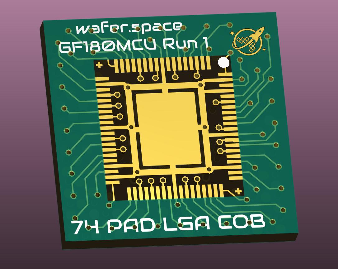
[
  {
    "description": "The wafer.space community is developing a flexible chip-on-board packaging strategy, so you won't need specialized equipment or expensive packaging services to use your chips.",
    "fields": [],
    "images": [],
    "inlineEmojis": [],
    "thumbnail": {
      "height": 863,
      "url": "2026-03_media/padframes-cob-lga-cob_png_open-graph-9D440.jpg",
      "width": 1086
    },
    "timestamp": null,
    "title": "Community Progress on Chip-on-Board Packaging Strategy",
    "url": "https://www.crowdsupply.com/wafer-space/gf180mcu-run-1/updates/chip-on-board"
  }
]{
"author": {
"avatarUrl": "2026-03_media/9679bb77da48d47c905b398d98a83780-75B68.png",
"discriminator": "0000",
"isBot": false
},
"message": {}
}message-1479950469483724851
2026-03-07T21:14:48.075+00:00 — J-Lo (@crockpotveggies)
- Message ID:
1479950469483724851 - Author ID:
591049455499739147 - Nickname: J-Lo
- User name: crockpotveggies
- Type:
Default - Discord message: https://discord.com/channels/1361349522684510449/1479540117101084803/1479950469483724851
- Archive source: https://discord.wafer.space/wafer-space/%E2%84%B9%EF%B8%8F%20-%20Information/%E2%81%89%EF%B8%8F-questions/multiple-pcb-design/2026-03/2026-03.json
- Archive source: https://discord.wafer.space/wafer-space/Information/questions/multiple-pcb-design/2026-03/2026-03.json
Content
@Tim 'mithro' Ansell thanks! I won’t claim to be an expert on packaging 🙂 I’ll have a read through this{
"author": {
"avatarUrl": "2026-03_media/a16190d2d5fede6615285958e112627c-CB61D.png",
"discriminator": "0000",
"isBot": false
},
"message": {
"inlineEmojis": [
{
"code": "slight_smile",
"id": "",
"imageUrl": "2026-03_media/1f642-83E8A.svg",
"isAnimated": false,
"name": "🙂"
}
],
"mentions": [
{
"avatarUrl": "2026-03_media/9679bb77da48d47c905b398d98a83780-75B68.png",
"color": null,
"discriminator": "0000",
"id": "169786952432746498",
"isBot": false,
"name": "mithro_",
"nickname": "Tim 'mithro' Ansell",
"roles": []
}
]
}
}message-1479953669792338043
2026-03-07T21:27:31.088+00:00 — tnt (@246tnt)
- Message ID:
1479953669792338043 - Author ID:
596068704471482370 - Nickname: tnt
- User name: 246tnt
- Type:
Default - Discord message: https://discord.com/channels/1361349522684510449/1479540117101084803/1479953669792338043
- Archive source: https://discord.wafer.space/wafer-space/%E2%84%B9%EF%B8%8F%20-%20Information/%E2%81%89%EF%B8%8F-questions/multiple-pcb-design/2026-03/2026-03.json
- Archive source: https://discord.wafer.space/wafer-space/Information/questions/multiple-pcb-design/2026-03/2026-03.json
Content
There are tons of companies that can package the dies in QFNs ... but expect something like ... say 20kEUR to package 500~1000 chips{
"author": {
"avatarUrl": "2026-03_media/88d17af9d19ab43565b0c46751ef7d12-DFEE5.png",
"discriminator": "0000",
"isBot": false
},
"message": {}
}