Category: 📐 - Designing
Parent channel: #🕰️-analog
Thread ID: 1534564700904226986
Messages: 9
message-1534567405492109392
2026-08-05T14:23:00.353+00:00 — tnt (@246tnt)
- Message ID:
1534567405492109392 - Author ID:
596068704471482370 - Nickname: tnt
- User name: 246tnt
- Type:
21 - Discord message: https://discord.com/channels/1361349522684510449/1534564700904226986/1534567405492109392
- Archive source: https://discord.wafer.space/wafer-space/%F0%9F%93%90%20-%20Designing/%F0%9F%95%B0%EF%B8%8F-analog/io-esd/2026-08/2026-08.json
Reply/reference
<details> <summary>Reference data</summary>{
"channelId": "1408135265427394661",
"guildId": "1361349522684510449",
"messageId": "1534564700904226986"
}Content
{
  "author": {
    "avatarUrl": "2026-08_media/88d17af9d19ab43565b0c46751ef7d12-DFEE5.png",
    "discriminator": "0000",
    "isBot": false
  },
  "message": {}
}message-1534567412681408664
2026-08-05T14:23:02.067+00:00 — tnt (@246tnt)
- Message ID:
1534567412681408664 - Author ID:
596068704471482370 - Nickname: tnt
- User name: 246tnt
- Type:
Default - Discord message: https://discord.com/channels/1361349522684510449/1534564700904226986/1534567412681408664
- Archive source: https://discord.wafer.space/wafer-space/%F0%9F%93%90%20-%20Designing/%F0%9F%95%B0%EF%B8%8F-analog/io-esd/2026-08/2026-08.json
Content
Ok, there are some small diodes on the input path after the resistor. But still, the main clamp are the actual drive transistors AFAICT.{
"author": {
"avatarUrl": "2026-08_media/88d17af9d19ab43565b0c46751ef7d12-DFEE5.png",
"discriminator": "0000",
"isBot": false
},
"message": {}
}message-1534570915252408443
2026-08-05T14:36:57.145+00:00 — Brunny (@brunny95)
- Message ID:
1534570915252408443 - Author ID:
693526428729344040 - Nickname: Brunny
- User name: brunny95
- Type:
Default - Discord message: https://discord.com/channels/1361349522684510449/1534564700904226986/1534570915252408443
- Archive source: https://discord.wafer.space/wafer-space/%F0%9F%93%90%20-%20Designing/%F0%9F%95%B0%EF%B8%8F-analog/io-esd/2026-08/2026-08.json
Content
The small diodes are standard (from what I've seen). Usually the path is: ESD main protections (GT mos or similar) - resistor - "small diodes" - core of the circuit{
"author": {
"avatarUrl": "2026-08_media/4f73efbb4824af137fec1ba3d7004c02-7FACC.png",
"discriminator": "0000",
"isBot": false
},
"message": {}
}message-1534571111357091971
2026-08-05T14:37:43.9+00:00 — Chips4Makers aka Staf Verhaegen (@chips4makers)
- Message ID:
1534571111357091971 - Author ID:
728516105680846892 - Nickname: Chips4Makers aka Staf Verhaegen
- User name: chips4makers
- Type:
Default - Edited: 2026-08-05T14:38:42.916+00:00
- Discord message: https://discord.com/channels/1361349522684510449/1534564700904226986/1534571111357091971
- Archive source: https://discord.wafer.space/wafer-space/%F0%9F%93%90%20-%20Designing/%F0%9F%95%B0%EF%B8%8F-analog/io-esd/2026-08/2026-08.json
Content
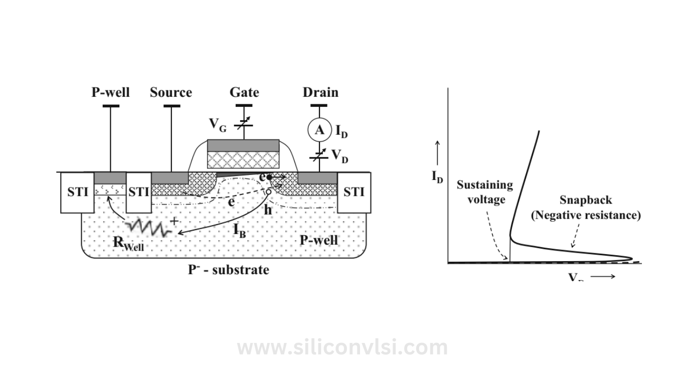
If properly designed output drivers can indeed also be used as ESD protection. This is using the so-called snap-back behavior. I believe [this](https://siliconvlsi.com/explain-the-snapback-phenomenon-in-nmos-devices/) should explain something. I used 0.18um TSMC when @imec and both IO NMOS and PMOS were designed to have that capability.Embeds
- Resolved media URL: https://siliconvlsi.com/explain-the-snapback-phenomenon-in-nmos-devices/
- Resolved media URL: https://discord.wafer.space/wafer-space/%F0%9F%93%90%20-%20Designing/%F0%9F%95%B0%EF%B8%8F-analog/io-esd/2026-08/2026-08_media/Snapback-mechanism-in-NMOS-1-5DD4E.png
[
  {
    "description": "The snapback phenomenon in NMOS devices is an important aspect in understanding their behavior and reliability.",
    "fields": [],
    "images": [],
    "inlineEmojis": [],
    "thumbnail": {
      "height": 768,
      "url": "2026-08_media/Snapback-mechanism-in-NMOS-1-5DD4E.png",
      "width": 1366
    },
    "timestamp": null,
    "title": "Explain the snapback phenomenon in NMOS devices - Siliconvlsi",
    "url": "https://siliconvlsi.com/explain-the-snapback-phenomenon-in-nmos-devices/"
  }
]{
"author": {
"avatarUrl": "2026-08_media/2649a6faac7843086b3d82b1d8f657a3-81998.png",
"discriminator": "0000",
"isBot": false
},
"message": {}
}message-1534571909847580734
2026-08-05T14:40:54.275+00:00 — Chips4Makers aka Staf Verhaegen (@chips4makers)
- Message ID:
1534571909847580734 - Author ID:
728516105680846892 - Nickname: Chips4Makers aka Staf Verhaegen
- User name: chips4makers
- Type:
Reply - Edited: 2026-08-05T14:41:15.494+00:00
- Discord message: https://discord.com/channels/1361349522684510449/1534564700904226986/1534571909847580734
- Archive source: https://discord.wafer.space/wafer-space/%F0%9F%93%90%20-%20Designing/%F0%9F%95%B0%EF%B8%8F-analog/io-esd/2026-08/2026-08.json
Reply/reference
<details> <summary>Reference data</summary>{
"channelId": "1534564700904226986",
"guildId": "1361349522684510449",
"messageId": "1534570915252408443"
}Content
It is known to me as secondary protection and the purpose is to get some extra voltage drop over the resistance during an ESD event to protect the connected gates.
The diode also has a capacitance so the R-C acts as a low-pass filter on the input though so high frequency stuff typically needs IO with custom ESD protection.{
"author": {
"avatarUrl": "2026-08_media/2649a6faac7843086b3d82b1d8f657a3-81998.png",
"discriminator": "0000",
"isBot": false
},
"message": {
"mentions": [
{
"avatarUrl": "2026-08_media/4f73efbb4824af137fec1ba3d7004c02-7FACC.png",
"color": null,
"discriminator": "0000",
"id": "693526428729344040",
"isBot": false,
"name": "brunny95",
"nickname": "Brunny",
"roles": []
}
]
}
}message-1534572435775422515
2026-08-05T14:42:59.666+00:00 — tnt (@246tnt)
- Message ID:
1534572435775422515 - Author ID:
596068704471482370 - Nickname: tnt
- User name: 246tnt
- Type:
Default - Discord message: https://discord.com/channels/1361349522684510449/1534564700904226986/1534572435775422515
- Archive source: https://discord.wafer.space/wafer-space/%F0%9F%93%90%20-%20Designing/%F0%9F%95%B0%EF%B8%8F-analog/io-esd/2026-08/2026-08.json
Content
Tx both, yeah I knew the secondary protection thing. But never heard of snapback.{
"author": {
"avatarUrl": "2026-08_media/88d17af9d19ab43565b0c46751ef7d12-DFEE5.png",
"discriminator": "0000",
"isBot": false
},
"message": {}
}message-1534680256223645878
2026-08-05T21:51:26.064+00:00 — Leo Moser (mole99) (@mole99)
- Message ID:
1534680256223645878 - Author ID:
323371864074485771 - Nickname: Leo Moser (mole99)
- User name: mole99
- Type:
Default - Discord message: https://discord.com/channels/1361349522684510449/1534564700904226986/1534680256223645878
- Archive source: https://discord.wafer.space/wafer-space/%F0%9F%93%90%20-%20Designing/%F0%9F%95%B0%EF%B8%8F-analog/io-esd/2026-08/2026-08.json
Content
Here are the ESD guidelines from the PDK: https://gf180mcu-pdk.readthedocs.io/en/latest/physical_verification/design_manual/drm_14_4.html
It seems like the snapback behavior is indeed used for ESD protection.{
"author": {
"avatarUrl": "2026-08_media/3c7c17f3225f6e56f4dccd83f14383f2-73F83.png",
"discriminator": "0000",
"isBot": false,
"roles": [
{
"color": null,
"id": "1423020172595298314",
"name": "Mod",
"position": 4
}
]
},
"message": {}
}message-1535352491695276072
2026-08-07T18:22:39.49+00:00 — namibj
- Message ID:
1535352491695276072 - Author ID:
262706220073222144 - Nickname: namibj
- User name: namibj
- Type:
Default - Discord message: https://discord.com/channels/1361349522684510449/1534564700904226986/1535352491695276072
- Archive source: https://discord.wafer.space/wafer-space/%F0%9F%93%90%20-%20Designing/%F0%9F%95%B0%EF%B8%8F-analog/io-esd/2026-08/2026-08.json
Content
There are ESD implants available specifically only for thick oxide area's sd-diffusion.{
"author": {
"avatarUrl": "2026-08_media/f885abc0dddd0a33e4d4991b3c99091d-7ACD2.png",
"discriminator": "0000",
"isBot": false
},
"message": {}
}message-1535353672127746128
2026-08-07T18:27:20.927+00:00 — namibj
- Message ID:
1535353672127746128 - Author ID:
262706220073222144 - Nickname: namibj
- User name: namibj
- Type:
Default - Discord message: https://discord.com/channels/1361349522684510449/1534564700904226986/1535353672127746128
- Archive source: https://discord.wafer.space/wafer-space/%F0%9F%93%90%20-%20Designing/%F0%9F%95%B0%EF%B8%8F-analog/io-esd/2026-08/2026-08.json
Content
There's also a trick were you employ something like a gate-triggered TRIAC that's constructed to bascially experience a safe and depending on details maybe or maybe-not power-cycle-requiring latchup to clamp the ESD voltage below what a passive diodes-to-PDN-rails arrangement could do, to be useful whenever thin-oxide devices are used to interact with pads.

An example that comes to mind would be e.g. DDR3 which is nominally 1.5V and fairly intense on the IO power draw due to combination of frequency, receive-side-termination, and ofc sheer wire count.{
"author": {
"avatarUrl": "2026-08_media/f885abc0dddd0a33e4d4991b3c99091d-7ACD2.png",
"discriminator": "0000",
"isBot": false
},
"message": {}
}